Applications

Substrates
Substrates
High-precision coatings are a prerequisite for precision optics. They make use of the interference properties and provide the desired characteristics.
Based on our experience, VON ARDENNE understands the physical processes that are necessary for vacuum coating of optical components. And we have the expertise in how to apply them to a multitude of different substrate shapes and sizes.

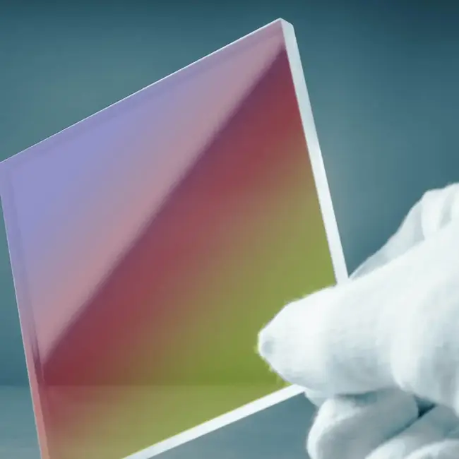
ULTRA-THIN GLASS
0.1 ~ 0.3 mm thick
Ø 200 mm

Wafer level optics
3D sensing
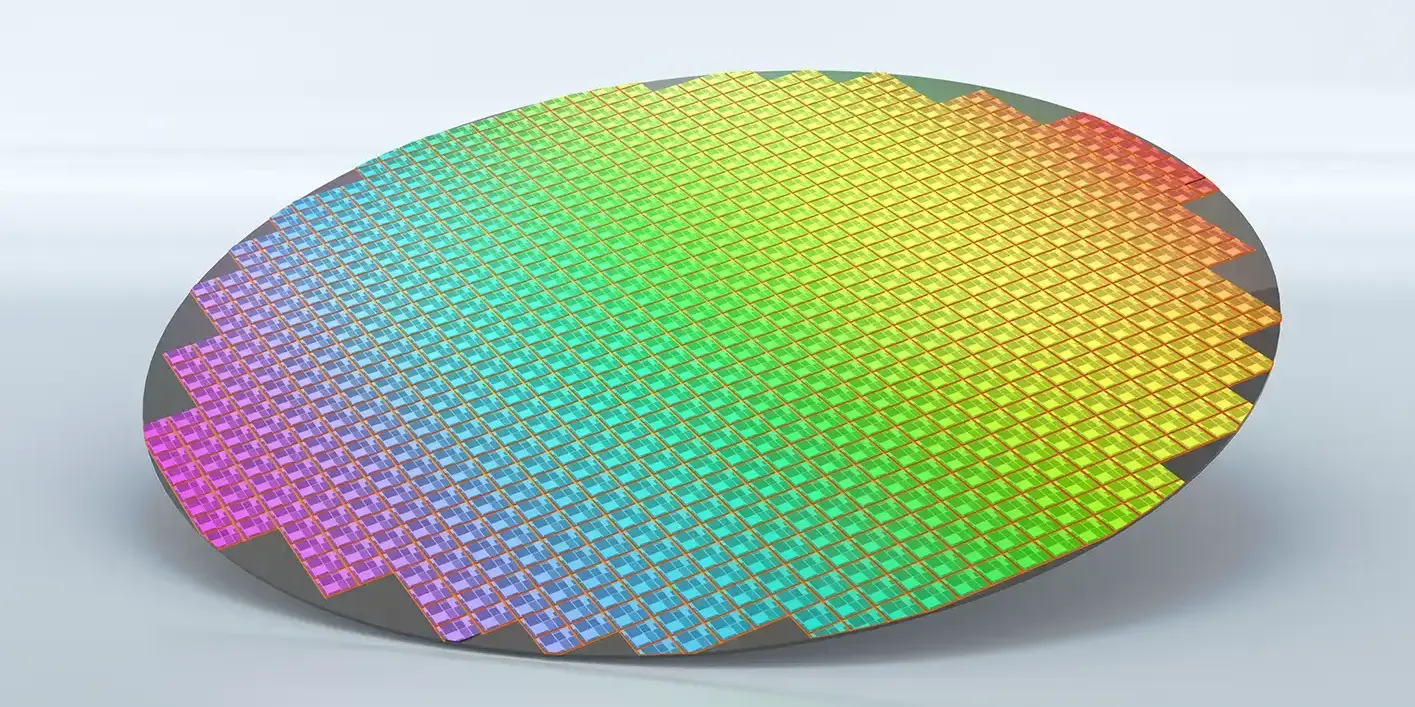
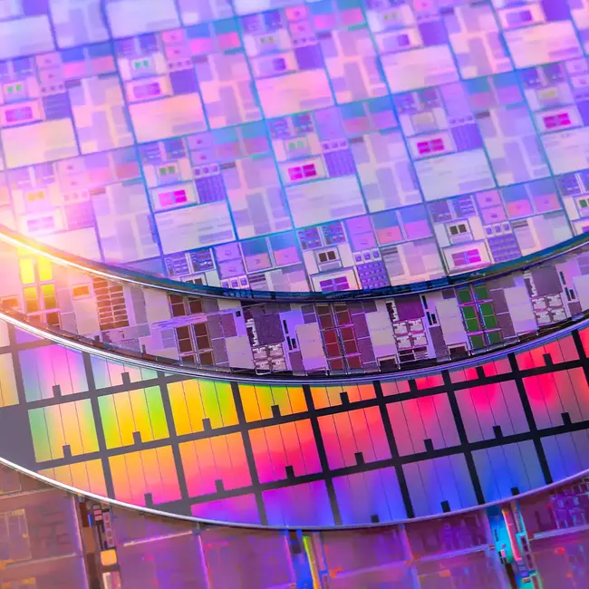
WAFERS (Si, InP, GaAs)
0.7 mm thick
Ø 4″, 6″, 200 / 300 mm
Wafer level optics
Laser diodes
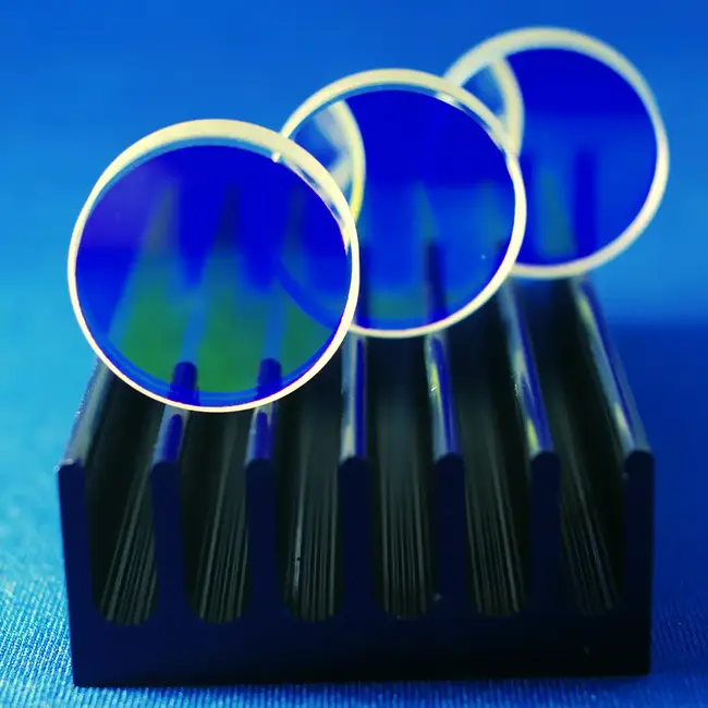
STANDARD
1.0 ~ 6.5 mm thick
Ø 1″, 2″, 25 / 50 mm
□ 50 x 50 mm2 / 100 x 100 mm2
Catalog optics
Laser optics
WEDGE-SHAPED
Like standards but with
nonparallel surfaces
(Δ << 1°)
Catalog optics
Laser optics
LARGE-AREA
2 ~ 50 mm thick
Ø up to 200 mm
□ up to 300 x 400 mm2
AV/VR/XR
Automotive, HUD
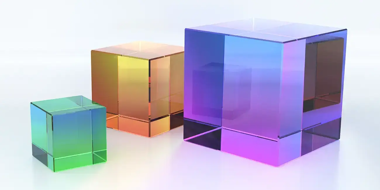
CUBICAL
5 x 5 x 5 mm³ up to
70 x 70 x 70 mm³
Telecom optics
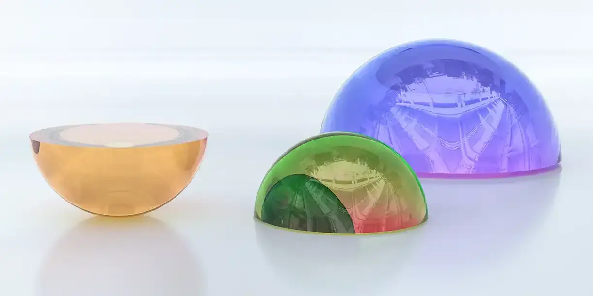
SPHERICAL
5 – 70 mm thick
Ø up to 200 mm
Laser optics
X-ray/EUV optics
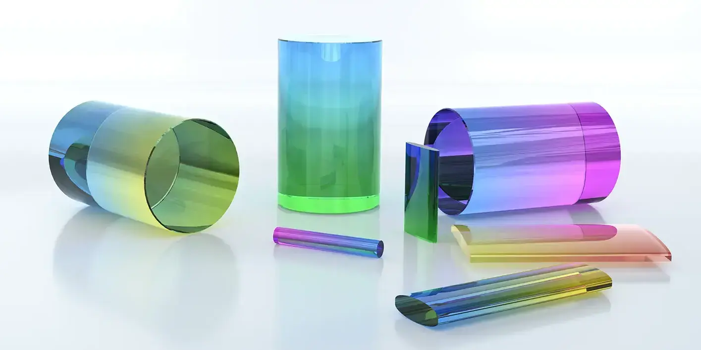
CYLINDRICAL
up to 70 mm thick
up to 200 mm wide
Laser optics
X-ray/EUV optics
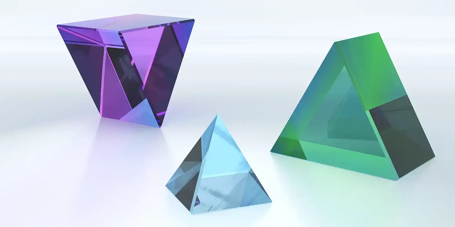
PRISMS
Up to 70 mm
edge length
Catalog optics
Periscope optics
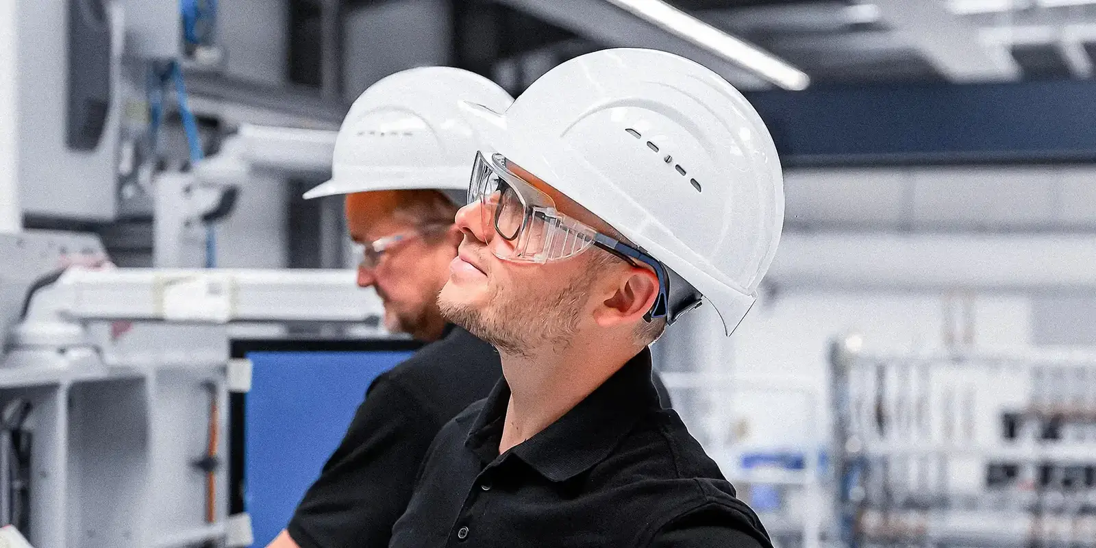
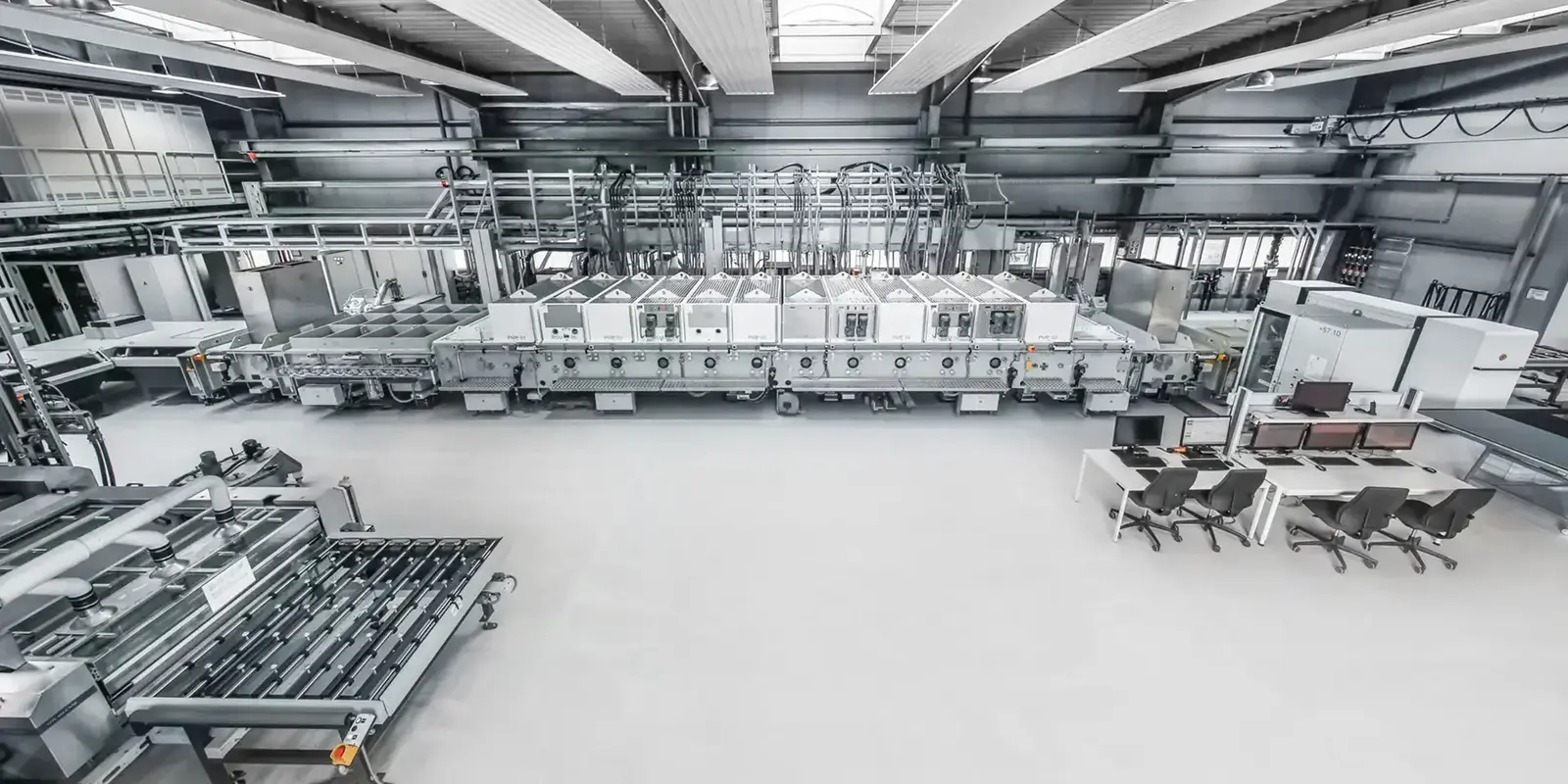
CLEANROOM
VA CLEANROOM
Cleanroom-Compatible Sampling & Assembly Facility
for precision optics, photonics & semiconductor applications
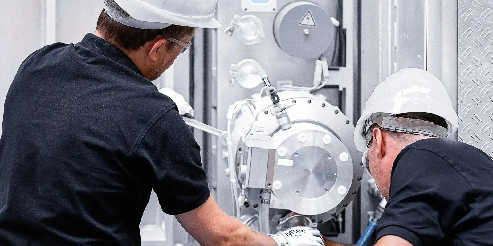
- Manufacturing of vacuum coating systems
- Sampling & pilot deposition services
- 600 m² semiconductor cleanroom including AMC capability
Support
Engineering
Simulation . Sampling . Layout
Technology & Application Center
Sampling . Development . Scaling
Service
Customer Portal . Spare Parts . Trainings
CONTACT
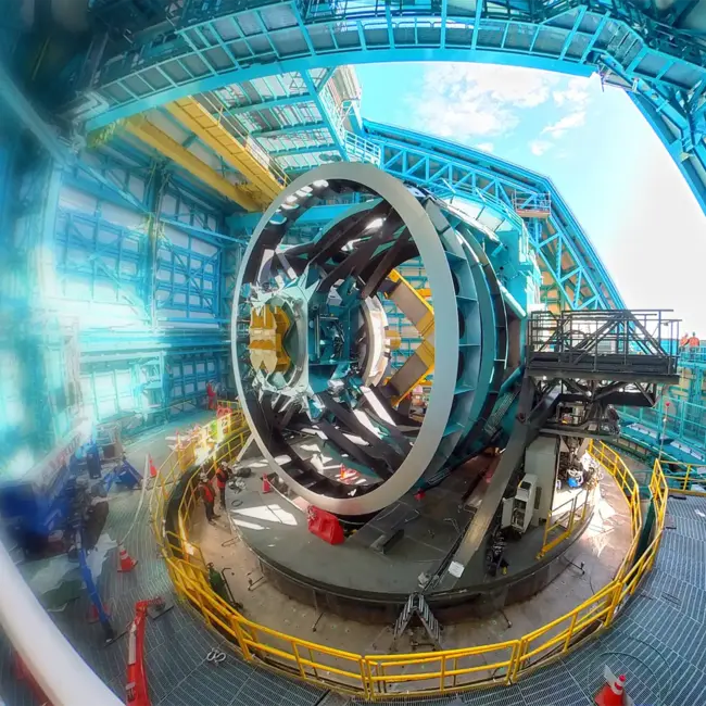
05.07.2026 - 10.07.2026
SPIE Astronomical Telescopes + Instrumentation 2026
Copenhagen, Denmark
Michael Schneider
Vice President Semiconductors & Precision Optics I Space & AviationVON ARDENNE GmbH